How Electron Microscopy & ToF Technology Transform Scientific Research
How Electron Microscopy and Time-of-Flight (ToF) Technology Enhance Scientific Research
Electron Microscopy (EM) and Time-of-Flight (ToF) technology are revolutionizing fields like nanotechnology, materials science, and biomedical research. Electron microscopy provides high-resolution imaging at the microscopic and even atomic levels, capturing intricate surface and internal details. However, traditional EM methods capture primarily 2D images, lacking depth information, which limits the ability to fully understand complex structures. ToF technology, which measures light travel time to provide highly accurate depth and spatial data, overcomes this limitation, offering a new dimension in microscopic imaging. By integrating ToF with EM, researchers now have the ability to capture not only surface features but also intricate 3D structures, improving precision in data analysis and scientific discovery.
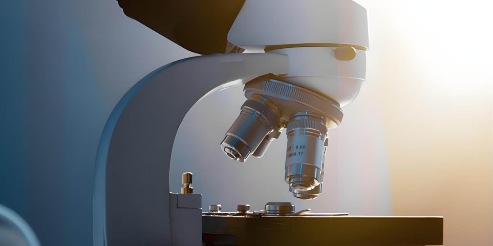
What is Electron Microscopy?
Electron microscopy uses electron beams to achieve much higher resolution compared to light-based methods. This allows scientists to study the fine details of materials, biological samples, and nanostructures. Two common types of electron microscopy are Scanning Electron Microscopy (SEM) and Transmission Electron Microscopy (TEM), both widely used for observing material compositions, cell structures, and semiconductor devices. However, traditional EM methods produce 2D images, which may not provide enough spatial context for certain applications, especially in fields like nanotechnology.
How Time-of-Flight (ToF) Technology Adds Depth to Electron Microscopy
ToF technology is a non-invasive 3D imaging technique that calculates the time it takes for light to travel to an object and back, providing accurate depth and distance data. This capability allows for the creation of detailed 3D models of objects, enhancing the overall understanding of their structures. In electron microscopy, ToF sensors can complement the high-resolution imaging of electron microscopes by providing depth information, turning 2D images into rich, three-dimensional reconstructions. This fusion opens up new possibilities for materials science, biomedicine, and semiconductor research.

How the Combination of EM and ToF Technology Transforms Research
When combined, electron microscopy and ToF technology offer several key advantages that push the boundaries of scientific research:
1. 3D Morphology Analysis
In materials science, the ability to analyze three-dimensional structures is crucial for understanding properties such as strength, conductivity, and thermal resistance. ToF technology enables the analysis of voids, cracks, and nanoparticle distributions, improving the design of materials used in various industries, from aerospace to electronics.
2. Dynamic Structural Monitoring
Traditional electron microscopes are static and can only capture single-frame images. By integrating ToF technology, researchers can track changes over time, making it easier to study how materials react under stress, temperature changes, or other external conditions. This is essential in industries like semiconductor research, where dynamic behavior at the nanoscale can impact device performance.
3. Defect Localization and Characterization
In industries such as semiconductor manufacturing, detecting tiny defects is essential. Traditional EM may miss internal flaws or fail to capture the full depth of issues. By adding ToF technology, defects can be more precisely located, enhancing the quality control process and reducing manufacturing errors.
4. 3D Imaging for Biological Research
In biomedical research, cells and tissues are inherently three-dimensional. Traditional 2D imaging cannot fully capture their structure. ToF-enhanced electron microscopy allows for clear 3D reconstructions of biological samples, aiding in studies of cellular dynamics, disease progression, and more effective diagnosis and treatment planning.

Enhancing Measurement Precision and Data Analysis
The combination of the depth data from Time-of-Flight (ToF) sensors with traditional 2D electron microscopy images creates powerful, rich, multidimensional models that provide a more comprehensive understanding of microscopic and nanoscale structures. By adding depth information to the surface details captured by electron microscopes, researchers can analyze intricate features that were previously hard to interpret. This integration significantly enhances the resolution of both surface topography and internal morphology, enabling precise measurements of complex structures. The synergy between 2D and 3D data allows for better characterization, enabling researchers to observe subtle variations, detect flaws, and gain insights into the dynamic behavior of materials and biological systems. Whether in nanomaterial analysis, biomedical imaging, or semiconductor inspections, this fusion of technologies allows researchers to make more accurate predictions, identify previously invisible defects, and create more detailed models of complex phenomena.
Key Applications of ToF-Enhanced Electron Microscopy
Semiconductor Manufacturing
In the highly precise world of semiconductor manufacturing, even the smallest defects can lead to significant performance issues. Traditional electron microscopes can provide high-resolution 2D images, but they often miss crucial 3D details that are critical for understanding internal structures. By integrating ToF technology into electron microscopy, manufacturers can accurately detect minute surface irregularities, such as scratches, cracks, or voids, as well as identify internal flaws like material inhomogeneities or stress points that might affect the performance of chips. This enhanced precision leads to higher-quality semiconductor devices and improved yield rates in chip production. With ToF-enhanced electron microscopy, manufacturers can ensure that every component meets rigorous industry standards, reducing the likelihood of product failures and improving overall efficiency in production processes.
Nanomaterial Characterization
The development of nanomaterials relies heavily on understanding their detailed properties at the microscopic and atomic levels. Traditional electron microscopy can reveal surface characteristics, but ToF technology adds an extra dimension by capturing 3D structures and internal configurations that are essential for evaluating the performance of these materials.
For example, ToF-enhanced electron microscopy allows researchers to analyze the distribution of nanoparticles within a composite material, examine the interfacial properties between nanomaterials, and study the arrangement of atoms within carbon nanotubes or graphene sheets. This deeper understanding helps to tailor materials for specific applications in electronics, energy storage, and biotechnology. With accurate 3D mapping of nanomaterial structures, scientists can optimize their designs for strength, conductivity, and thermal properties, pushing the boundaries of innovation in material science.
Biomedical Applications
In the biomedical field, understanding the three-dimensional structure of cells, tissues, and organs is essential for advancing diagnostics and treatment strategies. ToF-enhanced electron microscopy allows researchers to obtain highly detailed 3D reconstructions of biological samples, providing a clearer view of cellular processes and interactions. This technology is particularly useful for mapping the structure of cancerous tissues, observing how cells divide, or studying the development of organs. By capturing internal features such as cellular organelles and the extracellular matrix, researchers can gain insights into diseases at a much finer scale.
This detailed information plays a critical role in drug development, enabling the identification of potential targets for therapies or the evaluation of how drugs interact with cellular structures. Furthermore, ToF-enhanced EM can also help track the progression of diseases, monitor the effects of treatments in real time, and improve personalized medicine strategies by visualizing how individual cells or tissues respond to various interventions.
In summary, the integration of ToF technology with electron microscopy not only enriches the depth of analysis but also expands the range of research applications, from semiconductor manufacturing and nanomaterial characterization to biomedical research. This powerful combination is transforming the way researchers explore, measure, and analyze the world at the microscopic and atomic levels, driving innovation across multiple scientific and industrial fields.
Future Prospects for ToF-Enhanced Electron Microscopy
The integration of ToF and electron microscopy is still in its early stages, but the potential applications are vast. As artificial intelligence (AI) and big data technologies continue to advance, they will likely play a significant role in automating and streamlining the data analysis process, enabling real-time monitoring and faster decision-making in research and industrial applications.
Furthermore, the continued development of ToF sensors will likely lead to even greater precision, allowing scientists to explore the atomic and molecular world with unprecedented detail and speed. This advancement has the potential to revolutionize fields such as non-destructive testing, precision manufacturing, and even real-time analysis of living biological systems.
Conclusion
By combining the high-resolution imaging power of electron microscopy with the depth and spatial data provided by ToF technology, researchers can gain a more complete and accurate understanding of the microscopic world. This synergy is transforming industries ranging from semiconductor manufacturing and nanotechnology to biomedicine and material science. As these technologies evolve, the potential for more precise, efficient, and impactful scientific discoveries is limitless, driving advancements in both research and industry.
IHaw Structured Light Camera P050 0.50M

After-sales Service: Our professional technical support team specializes in TOF camera technology and is always ready to assist you. If you encounter any issues during the usage of your product after purchase or have any questions about TOF technology, feel free to contact us at any time. We are committed to providing high-quality after-sales service to ensure a smooth and worry-free user experience, allowing you to feel confident and satisfied both with your purchase and during product use.
-
Posted in
P050


Please upload banner from store admin blog pages