How Semiconductor Chips Enhance TOF Technology in Smart Devices
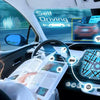
Semiconductor chips are pivotal in the development and functionality of Time-of-Flight (TOF) technology, which plays a crucial role in various smart applications like autonomous driving, robotics, augmented reality (AR), and virtual reality (VR). This article explores how semiconductor chips empower TOF sensors, making them more accurate, efficient, and adaptable across industries.
What Are Semiconductor Chips?
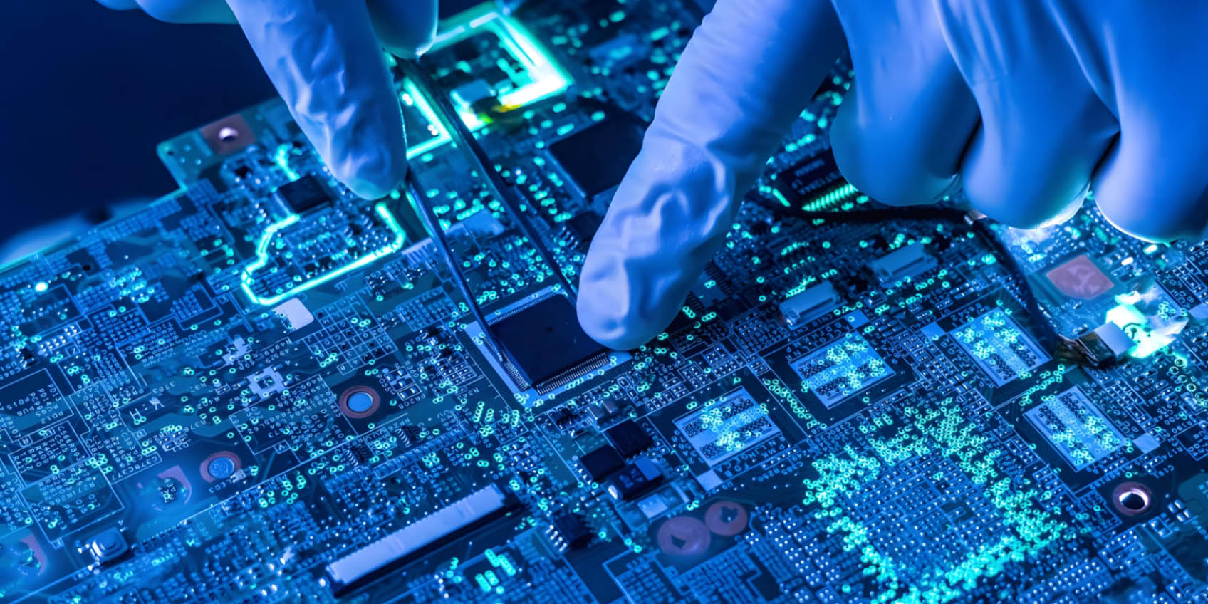
Semiconductor chips are essential electronic components made from semiconductor materials such as silicon and gallium arsenide. These chips allow precise control of current flow, a characteristic vital for most modern electronic devices. Semiconductor chips are at the heart of smartphones, computers, autonomous vehicles, and various smart devices. In the context of TOF technology, semiconductor chips are responsible for emitting and receiving signals and processing the data to generate accurate 3D measurements.
The Role of Semiconductor Chips in TOF Technology
TOF technology relies on the fundamental principle of measuring the time it takes for light to travel to an object and back, determining its distance. Semiconductor chips are integral to this process, ensuring that the system can emit and detect light signals with precision. Below are the key semiconductor components used in TOF systems:
-
VCSEL Chips (Vertical Cavity Surface Emitting Laser)
VCSEL chips act as light sources in TOF sensors, emitting high-power, stable laser pulses essential for accurate distance measurement. Compared to traditional LED light sources, VCSEL chips offer superior power consumption, precision, and stability. -
CMOS/CCD Image Sensor Chips
CMOS or CCD sensors receive the reflected light signals and convert them into electrical signals. These sensors are optimized for low-light conditions, enabling TOF technology to perform accurately in various lighting environments, such as at night or in dimly lit spaces. -
SPAD Chips (Single-Photon Avalanche Diode)
SPAD chips are highly sensitive and capable of detecting individual photons. Their ability to measure ultra-low light levels makes them ideal for high-precision depth sensing in environments with minimal light. -
AI Computation Chips (NPU, ASIC, FPGA)
To handle the massive amount of data produced by TOF sensors, AI chips such as NPUs, ASICs, and FPGAs perform rapid real-time processing of depth data. This enables TOF sensors to deliver quick, high-precision 3D maps in applications like autonomous driving and robotics.

Key Breakthroughs Through Semiconductor Integration
-
Enhanced Precision and Speed
The combination of high-precision VCSEL chips and SPAD sensors allows TOF systems to achieve millimeter or even micron-level depth measurement. This results in faster and more accurate 3D scanning, ideal for real-time applications like AR and autonomous navigation. -
Low Power Consumption
Advanced semiconductor processes (e.g., 5nm and 3nm) have enabled the development of power-efficient chips that extend the battery life of devices utilizing TOF sensors, such as smartphones, wearables, and drones. This ensures optimal performance while conserving energy, a crucial feature for portable devices. -
Improved Environmental Adaptability
TOF technology, powered by advanced semiconductor materials such as silicon carbide (SiC) and gallium nitride (GaN), is now capable of operating in extreme environmental conditions. These materials enhance TOF sensors’ ability to function in bright sunlight, low light, smoke, or rain, making them versatile for autonomous driving and other complex scenarios.

Future Developments in TOF Technology Driven by Semiconductor Chips
-
Higher Precision and Longer Range
Future TOF systems are set to incorporate nano-scale optical components, achieving even finer precision and supporting longer measurement ranges (over 100 meters). This would expand the use of TOF technology in areas like industrial automation, satellite mapping, and large-scale environmental monitoring. -
More Compact and Energy-Efficient Design
With the advent of 3nm and 2nm semiconductor fabrication processes, TOF sensors will become more compact and energy-efficient, making them suitable for a wider range of devices, including wearables and consumer electronics. -
Enhanced AI Integration
As AI chips and deep learning algorithms become more sophisticated, future TOF sensors will be able to perform more complex tasks, such as real-time 3D scene reconstruction, automatic object classification, and predictive analytics. This will revolutionize applications in autonomous vehicles, security, and AR/VR.

The Future of TOF Technology in a Semiconductor-Driven World
The combination of semiconductor chips and TOF technology is pushing the boundaries of what’s possible in 3D sensing and real-time data processing. As semiconductor advancements continue to accelerate, TOF systems will become more precise, efficient, and ubiquitous, transforming industries from autonomous driving to healthcare and beyond.
In conclusion, semiconductor chips form the backbone of TOF technology, enabling high-precision depth sensing, faster data processing, lower power consumption, and adaptability to complex environments. As these technologies continue to evolve, TOF sensors will become an indispensable part of our smart devices, driving innovation and efficiency across a wide range of industries.
SL90 Structure Light RGB-D Depth Camera

After-sales Service: Our professional technical support team specializes in TOF camera technology and is always ready to assist you. If you encounter any issues during the usage of your product after purchase or have any questions about TOF technology, feel free to contact us at any time. We are committed to providing high-quality after-sales service to ensure a smooth and worry-free user experience, allowing you to feel confident and satisfied both with your purchase and during product use.
-
Posted in
SL90


Please upload banner from store admin blog pages